General PCB layout guidelines
4-bit ETM trace
Arm Cortex-M devices have only a 4-bit ETM trace port. These trace signals must be routed to the standard 0.05 in × 0.05 in (1.27 mm × 1.27 mm) MIPI-20 connector header.
The recommended part number for a 4-bit ETM+JTAG debug connector is SHF-110-01-L-D-SM by Samtec or any other compatible shrouded header. The header should be positioned relatively close to the MCU—not more than 3 inches (75mm)—so that the even pins face the MCU as they have active signals on them.
16-bit ETM trace
Most Arm Cortex-R and Cortex-A devices come with a 16-bit trace port. To accommodate faster speeds, the signals must be connected to a 38-pin Mictor connector, making sure the track lengths from the MCU are matched to be within 0.5 inches (12.5 mm) to minimize signal skew.
The recommended part number for a 16-bit ETM+JTAG debug connector is 5767110-1 from AMP/Tyco.
The Mictor connector is designed to carry high-speed signals (10 Gb/s) and has a characteristic impedance of 50 Ohm. To eliminate signal distortion, the ETM trace signals on PCB must also have 50 Ohm impedance. The connector should be placed relatively close to the MCU—not more than 3 inches (75mm).
N-Trace
For RISC-V N-Trace, the same guidelines as above apply for 1-, 2-, 4-, and 16-bit trace ports. For details, see the RISC-V Trace Connectors Specification from the RISC-V N-Trace Task Group.
PCB routing
These are useful hints for PCB routing:
Use series termination
Place a series resistor on each trace signal near the source (MCU).
Minimize crosstalk
Keep all high-speed (fast rise and fall times) signals away from other signals to minimize crosstalk. Take special care of the TRACECLK signal.
Minimize signal skew
Keep the individual trace port track lengths to be within 0.5 inches (12.5mm) of each other.
Match impedance
Make the trace signal impedance 50 Ohm to match the impedance of the debug connectors and the debug probes.
Minimize signal vias and avoid track stubs
They might cause impedance mismatch, signal reflections, and distortions.
Avoid trace pin multiplexing
Multiplexing of the trace pins with other functions increases track lengths and adds capacitance and inductance and should be avoided. If multiplexing is required, the designer should add jumpers to disconnect the trace pins from the other logic in case the tracing signals are too distorted to function properly.
Use ground and power planes
Using ground and power planes not only helps with power distribution, but also gives the high-speed signals the shortest return path to ground, which results in less signal loss. They also make the trace impedance matching easier and more consistent.
Trace signal requirements
I-jet Trace supports DDR (Double Data Rate) clocking mode, which means the data is output on both edges of the TRACECLK signal. To compensate for variations in MCU trace logic and target board PCB layouts, I-jet Trace contains logic to delay the TRACECLK and each TRACEDATA signal for up to 2.5 ns in 78 ps steps (78.125 ps steps to be exact). This logic is used to synchronize all trace data lines with the trace clock automatically to get the optimum trace data collection.
Data setup and hold
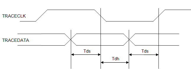
The following graph and table show the minimum setup and hold timing requirements of the trace signals with respect to TRACECLK. These timings are fixed by the MCU manufacturers, and might differ substantially from the data below, so are given as an example only.
Parameter | Value | Description |
|---|---|---|
Tds | 0.75 ns (minimum) | Data setup time |
Tdh | 0.75 ns (minimum) | Data hold time |
Important
The minimum setup and hold times in the table are not as important as the length of the data valid time, because the logic inside the I-jet probe can delay the TRACECLK and TRACEDATA signals as needed, up to 2.5 ns. To get the best results, the trace valid data (Tds + Tdh) should be as long as possible. The best way to achieve that in the MCU or ASIC, is to make sure the trace data is changed in the middle of the High or Low DDR TRACECLK signal. This way the trace data valid time is the widest and the data setup and hold times are the biggest for a given frequency.
Switching thresholds
I-jet Trace measures the target signals reference voltage (VTref) at the debug connector and automatically adjusts its switching thresholds to ½ of VTref. For example, on a 3.3 V target system, the switching thresholds are set to 1.65 V.